Product news
Cost-effective housing for IR emitters
May 20, 2026

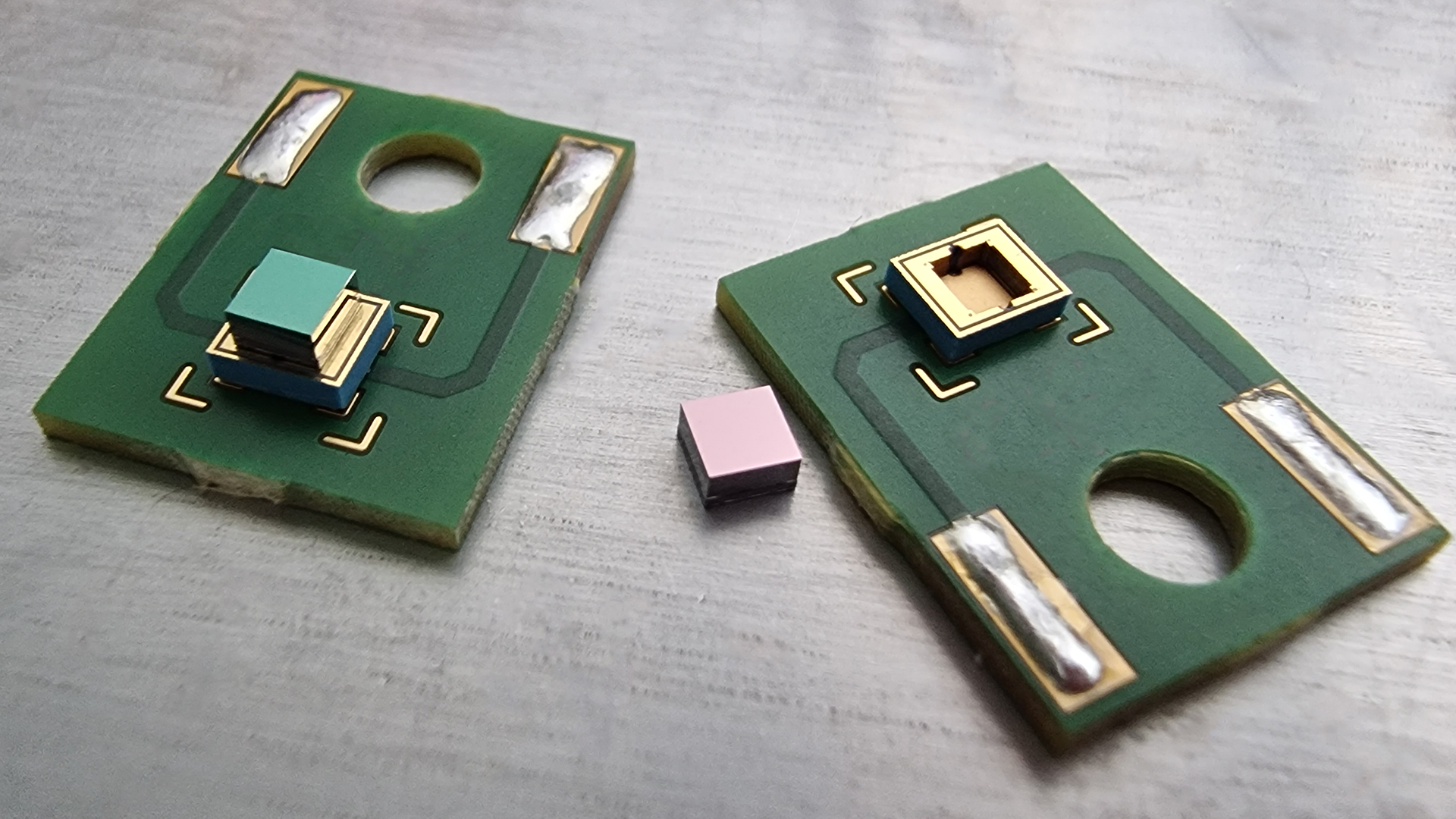
Excellent component properties are not enough—it is only through the use of appropriate assembly and housing technology that these parameters can be fully utilized. In the case of thermal infrared emitters, the package must fulfill several essential functions at once. These include, for example, sealing, optical filters or windows, heat dissipation, and the ability to be easily integrated into circuits and electronic sensor systems.
As part of the KHIS research and development project, a scalable housing platform for MEMS-based IR emitters was developed. An SMD-compatible package was developed on conventional FR4 circuit board material as well as on ceramic substrates (LTCC), which can be flexibly adapted to different emitter sizes. The key advantages of the new housing platform lie in its customizable size, reduced processing costs due to SMD technology, and a significantly smaller, cost-effective window or filter area. Optical windows are a significant cost factor, particularly in the mid-infrared range. In addition, a new emitter design was developed that, thanks to a flip-chip configuration, doubles the radiative power above 6 µm—a decisive advance for applications in the “fingerprint” analysis of many organic gases and liquids.
